
[ad_1]
One thing to look ahead to: Why has Intel chosen to make the massive strategic pivot and funding to not solely make chips for itself – because it’s at all times completed – however open up their factories to fabricate chips for different firms? It is a significantly vexing query for the corporate as a result of they did strive the chip foundry mannequin – constructing chips for different firms – and it failed on two earlier events.
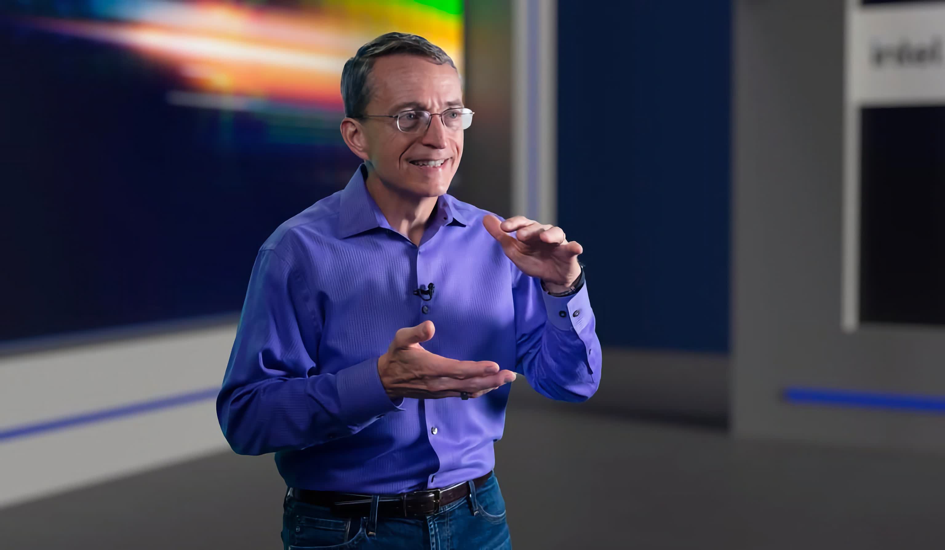
Upfront of the corporate’s first occasion devoted to their Intel Foundry enterprise taking place this week referred to as IFS Direct Join, I had the chance to sit down down one-on-one with Intel CEO Pat Gelsinger to get a way of what his and the corporate’s strategic objectives are in making this daring transfer.
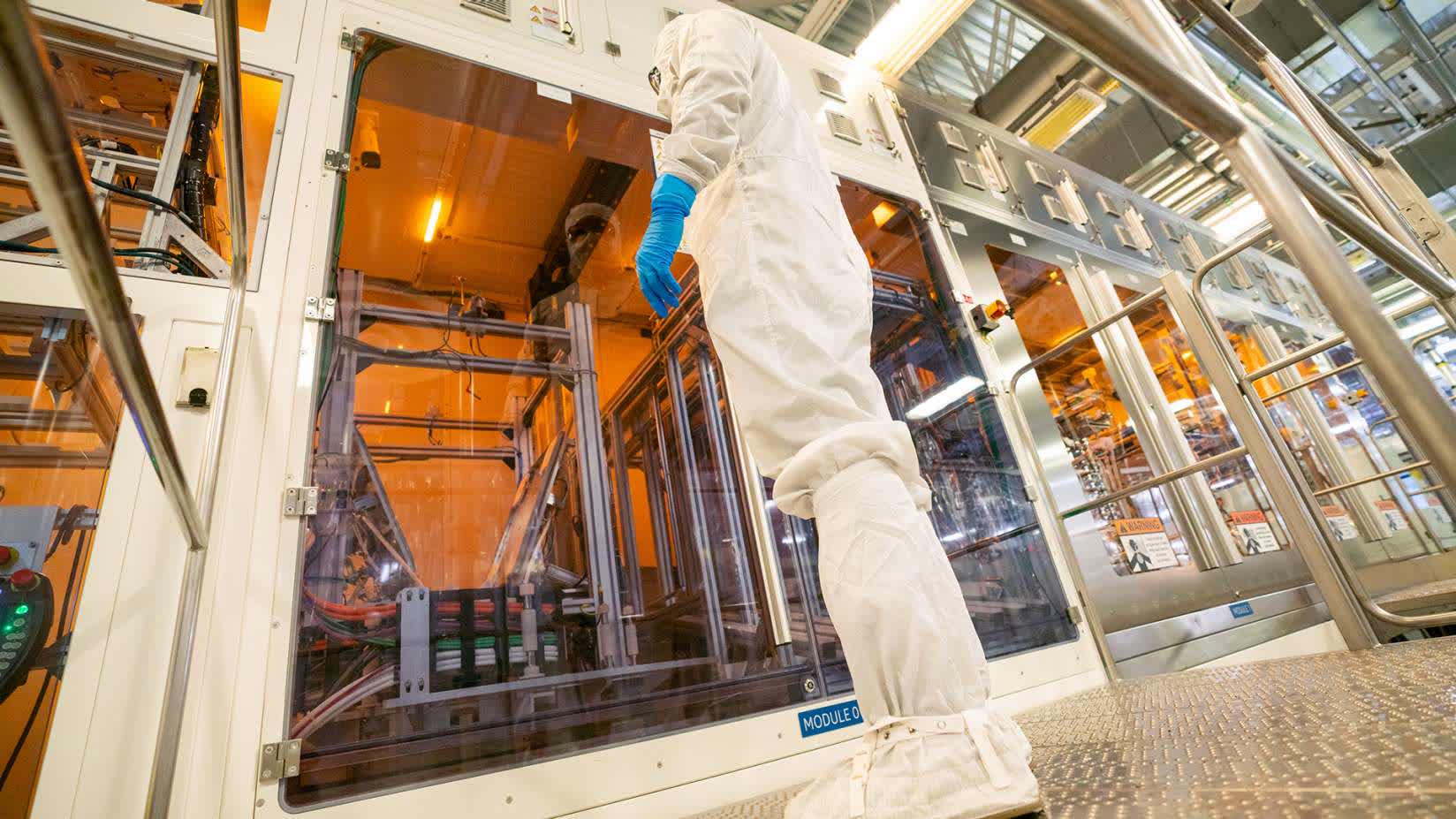
It seems packaging expertise – which permits the combining and interconnecting of a number of smaller chiplets into bigger, extra subtle SoCs – is a key a part of it. As Gelsinger associated, “[We’re doing] correct wafer on wafer stage meeting applied sciences with very superior capabilities. We have been working in these areas for many years and our management right here is hastily very fascinating.”
Based mostly on the spectacular array of audio system that Intel has scheduled for the occasion, together with Microsoft CEO Satya Nadella, Arm CEO Rene Haas, OpenAI CEO Sam Altman, US Secretary of Commerce Gina Raimondo, and executives from MediaTek, Broadcom, UMC, Cadence, Synopsys and extra, there’s clear trade pleasure across the new sources that the Intel Foundry is bringing to market. There have been even hints of some potential surprises popping out of IFS Direct Join.
Intel and Gelsinger refer to those sorts of capabilities as a system-level foundry. The thought is that in a world of more and more subtle chip designs, it takes much more than the newest and smallest course of applied sciences to place collectively probably the most subtle and strongest semiconductors.
“What we discovered was everyone wanted superior packaging,” Gelsinger mentioned, “so as an alternative of this simply being one thing that we will do, it is grow to be a foundational providing.”
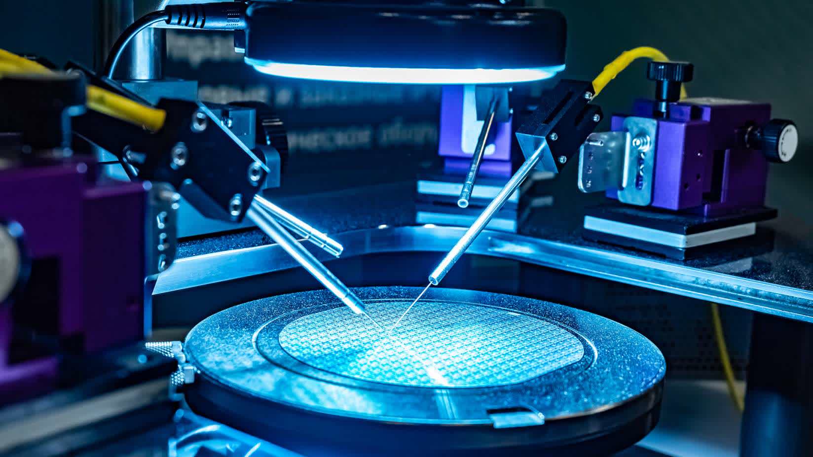
After all, Intel has made progress on the standard course of developments. The corporate is predicted to debate the state of the aggressive “5 nodes in 4 years” (5N4Y) initiative it began two years in the past at this week’s occasion. The important position of packaging, interconnect and different parts that permit the creation of “programs of chips,” nonetheless, is the place the corporate gives some distinctive benefits and a few essential alternatives.

“Why cannot Nvidia at this time do 2X the variety of GPUs the world desires?,” Gelsinger opined. “It isn’t due to silicon, it is due to packaging.”
Within the case of superior AI accelerator chips that the world is probably going going to wish giant portions of quickly, a few of these packaging capabilities and this system-level considering are going to be significantly essential Gelsinger mentioned.
“The AI chips of the long run may have multilayer 3D packaging with cache and reminiscence arrays and chiplets on high,” he famous. “I most likely wish to join these chiplets along with some type of UCIe by way of some hybrid bonding or one thing like that onto a base chip as nicely,” he continued. “I [also] must have all the drivers, the bottom stage capabilities related to that software program to compose this factor. These are simply a few of the examples of what it takes to be that subsequent era system foundry.”
Inherent in Gelsinger’s feedback is the corporate’s willingness to share each IP and experience it has developed in creating its personal chips with foundry clients. “Our consumer designs have been doing this [advanced package design] already and we’re making that experience of methods to compose these absolutely obtainable as a part of the foundry service choices.”
That is a part of the adjustments that Gelsinger has made on this newest try to construct a foundry enterprise inside Intel. As well as, the corporate has completed work to combine rather more simply with the whole chip design trade, significantly with EDA software program firms like Cadence and Synopsys. “Up to now, Intel was at all times tremendous proprietary,” Gelsinger mentioned. “You needed to bounce over this big quantity of effort [to learn] all of our proprietary instruments and flows. That is why the Cadence and Synopsys relationships are so essential.”
Whereas Gelsinger freely admitted that it was nonetheless too early to inform, he did recommend that the approaches they’re taking and the emphasis on packaging and programs design they’ve are shifting them previous earlier foundry efforts. “We have mentioned we’re over $10 billion in lifetime deal worth and that is multiples of what it was prior to now. We’re additionally well past the quantity of income, clients, and so on., that was ever a part of these earlier efforts.”
Along with the sensible demand and design necessities for superior packaging applied sciences, Gelsinger additionally identified how the economics of contemporary chip design and manufacturing are evolving.
“If we might return 5 years for a modern CPU, within the Invoice of Supplies, 15% [of the cost] could be for package deal meeting and take a look at. As we get to one of many trendy chips, like Gaudi [an Intel AI Accelerator chip] or Granite Rapids [a future Intel server CPU], which can be utilizing these 3D building applied sciences, package deal meeting and take a look at is now 35 to 40%. So, the entire worth of the product is turning into rather more, seen by way of the package deal meeting and take a look at layers.”
After all, one more reason the corporate is pursuing this foundry mannequin is because of each the stunning lack of geographical manufacturing variety within the chip enterprise and the stark actuality of at this time’s geopolitical setting.
At current, over 50% of all of the world’s semiconductors and about 90% of probably the most superior chips are inbuilt Taiwan by TSMC, USMC and others. The issue is that China has not too long ago been elevating a number of pink flags hinting at a possible invasion and takeover of Taiwan, a rustic that it believes continues to be a part of China. On high of that, Taiwan sits alongside the notorious Ring of Fireplace, a tectonic belt surrounding a lot of the Pacific Ocean that’s recognized for the form of earthquake exercise that might wreak havoc on the nation’s infrastructure.
The online end result has been a wakeup name heard around the globe in regards to the tremendously essential must geographically diversify the place chips are made. Lengthy-time semiconductor trade observers have been making this level for many years, however the chip shortages in merchandise like automobiles that occurred throughout the pandemic shone an intense new mild on the issue.
Consequently, governments have began to create big applications to financially help home chip manufacturing exercise – together with the $52 billion CHIPS Act right here within the US, which has simply began to dole out its first funds.
Not surprisingly, Gelsinger desires to benefit from these funds not simply due to the plain financial windfall however due to the necessity to get the US, Europe, and different components of the world in a stronger place from a chip manufacturing perspective. “[Asian] governments closely backed [the semiconductor industry] for 3 a long time, and now we’re 80% depending on Asia,” he mentioned. “If we’ll deliver it again, we’ve got to shut the financial hole, proper?”
Sadly, the method of getting these funds has confirmed to be slower than anticipated. Gelsinger commented, “After I stood on the White Home garden on the signing of the invoice in August of 2022, did I believe I might be sitting right here speaking to you at this time, and say, I have never seen a penny but? No.” These funds are important too as a result of as Gelsinger identified, “We’re making investments with the presumption that these grants, tax credit, and so on., materialize.”
In the long run, Gelsinger is optimistic in regards to the efforts, however time is of the essence. “I really feel like I’ve a dedication from Congress right here and a dedication from Parliament and the EU, however you already know, sooner or later the [Intel] board’s gonna say, OK, Pat, sufficient’s, sufficient.”
Authorities subsidies apart, it takes much more than opportunism to construct a profitable foundry enterprise and Gelsinger is aware of it.
Intel cannot make a critical run at it with out having the sorts of chip manufacturing competencies that different firms wish to use. Finally, it is these distinctive capabilities in packaging and chip programs design, in addition to a purpose-driven strategy that may make or break the audacious plan upon which Gelsinger and Intel have embarked.
It is clearly not a simple objective, however it’s one he appears pushed to attain.
Bob O’Donnell is the founder and chief analyst of TECHnalysis Analysis, LLC a expertise consulting agency that gives strategic consulting and market analysis providers to the expertise trade {and professional} monetary group. You possibly can comply with him on X @bobodtech
[ad_2]
Source link


